E-mail
Jiaxing AOSITE Photonics Technology Co.,Ltd.
inas substrate
inas substrate

OST Photonics InAs Substrates

With InAs single crystal substrate, InAsSb/In-AsPSb, InNAsSb and other heterojunction materials can be grown to produce infrared light-emitting devices with wavelengths of 2-14μm. InAs single crystal substrates can also be used to epitaxially grow AlGaSb superlattice structure materials. Mid-infrared quantum cascade laser. These infrared devices have good application prospects in gas monitoring, low-loss optical fiber communications and other fields. In addition, InAs single crystal has high electron mobility and is an ideal material for making Hall devices. As a single crystal substrate, InAs materials need to have low dislocation density, good lattice integrity, appropriate electrical parameters and high uniformity. The main growth method of InP single crystal materials is the traditional liquid-sealed Czochralski technology (LEC).


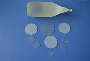
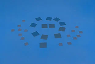
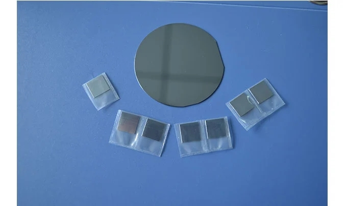
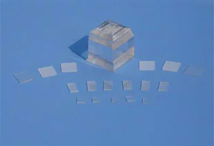
OST Photonics offers high quality InAs substrates for researchers and industries. There are four types of InAs materials for you to choose from: N-type InAs (undoped), N-type InAs (Sn doped), N-type InAs (S doped) and P-type InAs (Zn doped). Crystal orientation, size and thickness can be customized according to your requirements.

Application of InAs Substrates


  • Optical fiber communication

  • High-speed and low power electronic devices

  • Infrared light-emitting devices

  • Mid infrared quantum cascade laser


Advantages of InAs Substrates


  • High electron mobility

  • Low magneto resistance effect

  • Small effective mass

  • Low resistance temperature coefficient


Ability of InAs Substrates


  • Orientation:<100>, etc.

  • Dimension: 2”, 3”, 10x10mm, 10x5mm, etc.

  • Thickness: 0.5mm, 0.6mm, etc.

  • Available items: wafers, substrates, blanks and customized optics


Specification and Properties of InAs Substrates


Crystal Structure

Cube

a=6.058 Å

Melting Point

942 ℃

Density

5.66 g/cm3

Band Gap

0.45

Doping

Undoped

Sn

S

Zn

Conduct Type

N-type

N-type

N-type

P-type

Carrier Concentration

5x10^16 cm-3

(5-20)x10^17 cm-3

(1-10)x10^17 cm-3

(1-20)x10^17 cm-3

Mobility

≥2x10^4 cm2/V.s

>2000 cm2/V.s

>2000 cm2/V.s

100-300 cm2/V.s

Dislocation Density

<5x10^4 cm-2

<5x10^4 cm-2

<5x10^4 cm-2

<5x10^4 cm-2

Orientation

<100>, etc.

Orientation Tolerance

±0.5° or better

Dimension

2”, 3”, 10x10mm, 10x5mm, etc.

Dimension Tolerance

±0.1 mm or better

Thickness

0.5mm, 0.6mm, etc.

Thickness Tolerance

±0.05 mm or better

Surface Finish

Single side polished (SSP)/Double sides polished (DSP)

Surface Roughness

Ra<5Å
Atomic Particle Microscopy (AFM) test report can be provided.

Package

Class 100 clean bag, Class 1000 super clean room


Contact Us
Welcome your presence, you can send us an email, we will get in touch with you within 24 hours.
Head Office: No. 66, 8 Group, Chengbei Village, Yanguan Town, Jiaxing 314411, China;

Hangzhou Branch: Room 1012, Chunhua Bussiness Center, No. 159, Hangbo Street, Shangcheng District, Hangzhou 310009, Zhejiang, China
Head Office: No. 66, 8 Group, Chengbei Village, Yanguan Town, Jiaxing 314411, China;

Hangzhou Branch: Room 1012, Chunhua Bussiness Center, No. 159, Hangbo Street, Shangcheng District, Hangzhou 310009, Zhejiang, China
sales@ostphotonics.com; info@ostphotonics.com +86-0571-86780460