E-mail
Jiaxing AOSITE Photonics Technology Co.,Ltd.
ce yag substrate
ce yag substrate
ce yag crystal substrates

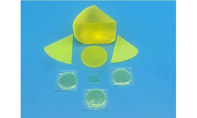
OST Photonics Ce YAG Substrates

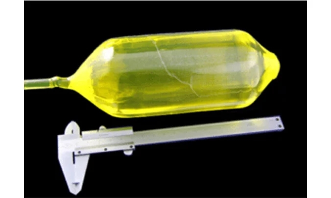
Ce:YAG is a scintillation crystal with high luminous efficiency and wide light pulse, and its luminous peak (550nm) can be well matched with the sensitive wavelength of the photodiode. It is suitable for use as a photo detector and charged particles light detection. It has non-deliquescent, high temperature resistant, stable thermodynamics, and can be used in extreme detection environments.


OST Photonics offers high quality Ce:YAG substrates for researchers and industries. Crystal size and thickness can be customized according to your requirements. Additionally, we are capable of providing Ce:YAG transparent ceramics with a maximum diameter of 8 inches and a maximum doping concentration of 20%, if you are interested in Ce:YAG transparent ceramics, please contact us!

Application of Ce YAG Substrates


  • Beta, X-ray counter

  • X-ray imaging screens

  • Electron imaging screens

  • Ion beam imaging

  • Scanning electron microscope(SEM)


Advantages of Ce YAG Substrates


  • High scintillating efficiency

  • Fast decay time

  • Stable physical and chemical properties

  • High thermal conductivity

  • Wavelength of peak emission well matched with the sensitive wavelength of the photodiode


Ability of Ce YAG Substrates


  • Orientation:<111>, etc.

  • Maximum Size: ɸ80mm x 200mm

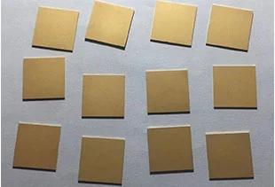
  • Dimension: 1”, 2”, 25x25mm, 10x10mm, 10x5mm, 5x5mm, etc.

  • Thickness: 0.5mm, 1.0mm, etc.

  • Available items: substrate, blanks, scintillation screen and customized optics


Specification and Properties of Ce YAG Substrates


Crystal System

Cubic

Crystal Lattice Constant

a=12.01Å

Density

4.55 g/cm3

Hardness

8.5 Mohs

Melt Point

1970 ℃

Thermal Expansion

7.8 x 10^-6 /℃

Orientation

<111>, etc.

Orientation Tolerance

±0.5° or better

Dimension

1”, 2”, 25x25mm, 10x10mm, 10x5mm, 5x5mm, etc.

Dimension Tolerance

±0.1 mm or better

Thickness

0.5mm, 1.0mm, etc.

Thickness Tolerance

±0.05 mm or better

Surface Roughness

Ra<5Å
Atomic Particle Microscopy (AFM) test report can be provided.

Surface Finish

Single side polished (SSP)/Double sides polished (DSP)

Package

Class 100 clean bag, Class 1000 super clean room


Contact Us
Welcome your presence, you can send us an email, we will get in touch with you within 24 hours.
Head Office: No. 66, 8 Group, Chengbei Village, Yanguan Town, Jiaxing 314411, China;

Hangzhou Branch: Room 1012, Chunhua Bussiness Center, No. 159, Hangbo Street, Shangcheng District, Hangzhou 310009, Zhejiang, China
Head Office: No. 66, 8 Group, Chengbei Village, Yanguan Town, Jiaxing 314411, China;

Hangzhou Branch: Room 1012, Chunhua Bussiness Center, No. 159, Hangbo Street, Shangcheng District, Hangzhou 310009, Zhejiang, China
sales@ostphotonics.com; info@ostphotonics.com +86-0571-86780460