E-mail
Jiaxing AOSITE Photonics Technology Co.,Ltd.
magnesium oxide crystal
mgo substrate

OST Photonics MgO Substrate

Magnesium oxide (MgO) single crystal substrates are widely used in many thin film technology fields. Such as the production of magnetic films, semiconductor films, optical films and high-temperature superconducting films. Because the dielectric constant and loss of MgO single crystal in the microwave band are very small, and large-area substrates (2 inches in diameter and larger) can be obtained, it is an important high-temperature superconducting thin-film single crystal substrate for the current industrialization. one. It can be used to make high-temperature superconducting microwave filters and other devices required by mobile communication equipment, and has a large realistic and potential application market.


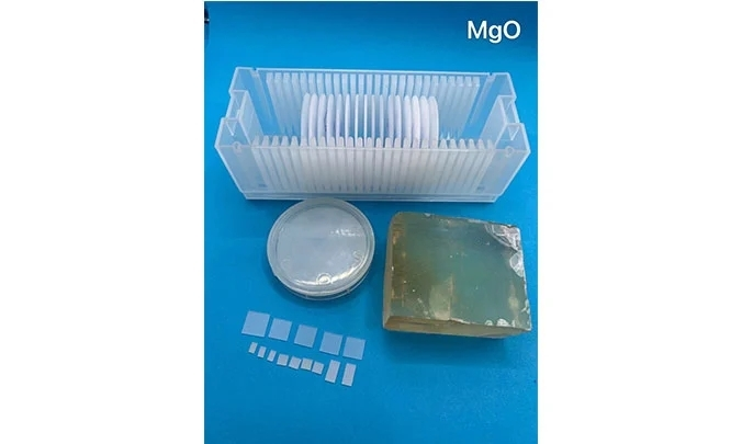
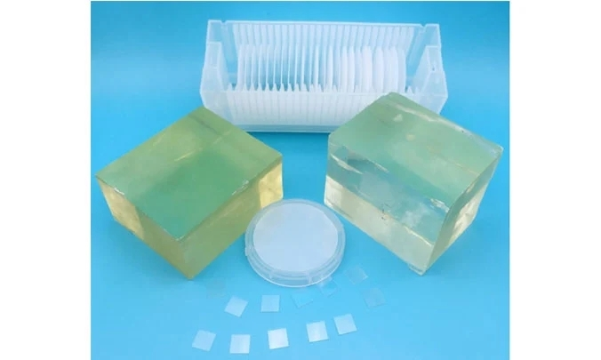
OST Photonics offers high quality MgO substrates for researchers and industries. Crystal orientation, size and thickness can be customized according to your requirements.

Application of MgO Substrate


  • High-temperature superconducting microwave filters

  • Substrate material for the magnetic film, semiconductor films, optical films, and high-temperature superconducting films


Advantages of MgO Substrate


  • Small dielectric constant and loss in the microwave band

  • High and low-temperature resistance

  • Good Corrosion resistance

  • Good thermal conductivity

  • Excellent optical properties


Ability of MgO Substrate


  • Orientation:<001>,<110>,<111>, etc.

  • Dimension: 1”, 2”, 5x5mm, 10x10mm, 20x20mm, 30x30mm, etc.

  • Thickness: 0.5mm, 1.0mm, etc.

  • Available items: wafers, substrates, blanks and customized optics


Specification and Properties of MgO Substrate


Crystal Structure

Cube

Growth Method

Special Arc Melting

Lattice Constant

a=4.130 Å

Melting Point

2800 ℃

Purity

>99.95%

Density

3.58 g/cm3

Hardness

5.5 Mohs

Thermal Expansion Coefficient

11.2×10^-6 /℃

Cleavage Plane

<100>

Optical Transmission

>90% (200~1000 nm)

Dielectric Constants

ε= 9.65

Thermal Conductivity

36 W/m.k @300K

Orientation

<001>,<110>,<111>, etc.

Orientation Tolerance

±0.5° or better

Dimension

1”, 2”, 5x5mm, 10x10mm, 20x20mm, 30x30mm, etc.

Dimension Tolerance

±0.1 mm or better

Thickness

0.5mm, 1.0mm, etc.

Thickness Tolerance

±0.05 mm or better

Surface Finish

Single-side polished (SSP)/Double sides polished (DSP)

Surface Roughness

Ra≤5Å (5µmx5µm)

Package

Class 100 clean bag, Class 1000 super clean room


Contact Us
Welcome your presence, you can send us an email, we will get in touch with you within 24 hours.
Head Office: No. 66, 8 Group, Chengbei Village, Yanguan Town, Jiaxing 314411, China;

Hangzhou Branch: Room 1012, Chunhua Bussiness Center, No. 159, Hangbo Street, Shangcheng District, Hangzhou 310009, Zhejiang, China
Head Office: No. 66, 8 Group, Chengbei Village, Yanguan Town, Jiaxing 314411, China;

Hangzhou Branch: Room 1012, Chunhua Bussiness Center, No. 159, Hangbo Street, Shangcheng District, Hangzhou 310009, Zhejiang, China
sales@ostphotonics.com; info@ostphotonics.com +86-0571-86780460