E-mail
Jiaxing AOSITE Photonics Technology Co.,Ltd.
optical grade lithium niobate wafer
optical grade linbo3 wafers
optical grade linbo3
optical grade lithium niobate

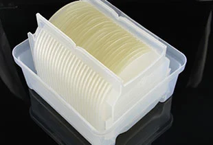
OST Photonics Optical Grade Lithium Niobate Wafers

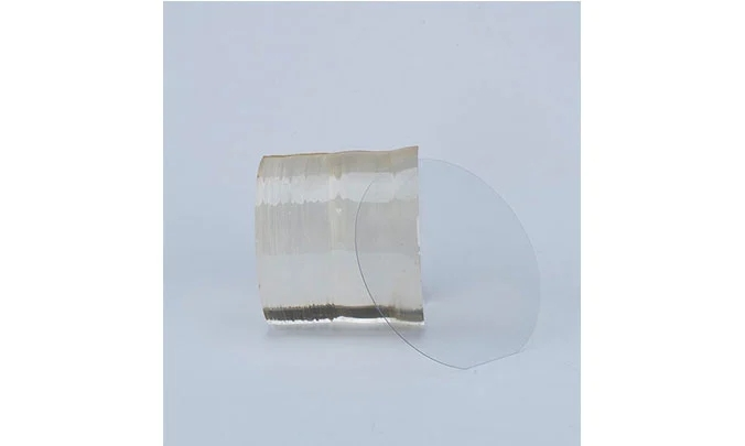
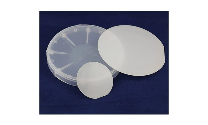
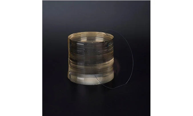
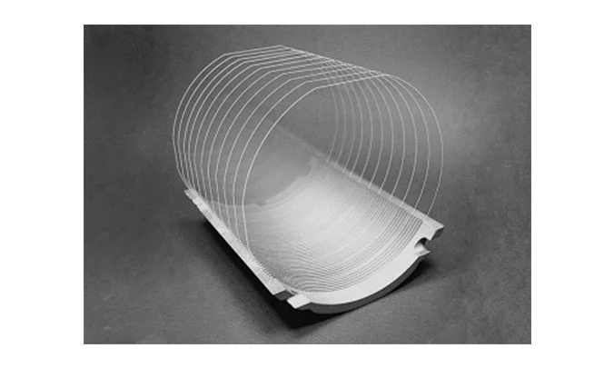
OST Photonics offers a variety of sizes and thicknesses of optical grade Lithium Niobate wafers(linbo3 wafers), with wafer diameters ranging from 2 inches to 4 inches, the thickness can be customized according to your requirements (generally above 0.18 mm). The orientations can be X/Y/Z etc. Congruent lithium niobate (CLN), near-stoichiometric lithium niobate (SLN), and Tm/Pr/Er/Fe/MgO doped lithium niobate wafers are also available upon request.

Application of Optical Grade Lithium Niobate Wafers


  • Optic Isolators

  • Periodically poled lithium niobate (PPLN) waveguides

  • EO Phase Modulators

  • Optical Modulator

  • Electro-optic Q-switches


Advantages of Optical Grade LiNbO3 Wafer


  • Stable mechanical properties

  • Good machinability

  • Heat and corrosion resistance

  • High electro-optic and high nonlinear optic coefficients


Ability of Optical Grade Lithium Niobate Wafers


  • Diameter: 2”, 3”, 4”

  • Orientations: X, Y, Z etc.

  • Thickness: 0.25mm, 0.5 mm, 1.0 mm etc.

  • Available items: crystal wafers, congruent lithium niobate (CLN) wafers, near-stoichiometric lithium niobate (SLN) wafers, Tm/Pr/Er/Fe/MgO doped LiNbO3 wafers, boules, blanks and customized optics


Product Parameters of Optical Grade Lithium Niobate Wafers


Material

LiNbO3 single crystal

Curie Temp

1142±2.0℃

Cutting Angle

X/Y/Z etc

Orientation Tolerance (±)

≤15′

Diameter

2”/3”/4”

Diameter Tolerance (±)

≤0.20 mm

Thickness

0.18 ~ 0.5mm or more

Thickness Tolerance (±)

≤0.025 mm

Primary Flat Length

16mm/22mm/32mm

TTV

<1~5 µm

BOW

± (25~40 um)

Warp

<= 35 µm

Orientation Flat

According to our standards or your requests

Surface Type

Single side polished(SSP)/double sides polished(DSP)/double sides lapped(DSL)

Polished Side Ra

<0.5nm

Polished Side Surface Quality

S/D 20/10

Lapped Side Ra

General is 0.2-0.5 um or as customized

Edge Criteria

Compliant with SEMI M1.2 Standard/refer to IEC62276

Quality

Free of crack (bubbles and inclusions)

Optical Doped

Er/Fe/MgO etc

Wafer Surface Criteria

Refractive index

No=2.2878/Ne=2.2033@632nm wavelength/prism  coupler method.

Contamination

None

Particles φ>0.3 um

<= 30

Scratch , Chipping

None

Defect

No edge cracks, scratches, saw marks, stains

Packaging

Qty/Wafer box

25pcs per box


Product Parameters of Optical Grade Lithium Niobate Wafers


Material

Grade

Diameter

Growth direction

LiNbO3

optical

2”/3”/4”

X/Y/Z/Y135 etc

MgO:LiNbO3

optical

2”/3”

X/Z

Fe:LiNbO3

optical

2”/3”

Z

Tm:LiNbO3

optical

2”/3”

Z

Pr:LiNbO3

optical

2”/3”

Z

Er:LiNbO3

optical

2”/3”

X/Z


Properties of Optical Grade Lithium Niobate Wafers


Growth method

Czochralski method

Crystal structure

M3

Lattice Constant

a=b=5.148 Å     c=13.863 Å

Melting point (℃)

1250

Density(g/cm3)

4.64

Hardness

5 (Mohs)

Refractive index

no=2.286 ne=2.203  at 632.8nm

Nonlinear coefficient

d33=34.45, d31=d15=5.95, d22=13.07 (pmv-1)

Electro-optical coefficient

γ13=8.6, γ22=3.4, γ33=30.8, γ51=28.0, γ22=6.00 (pmv-1)

Optical transmittance

370 ~ 5000nm and >68% at 632.8nm

Thermal expansion

a11=15.4x10^-6/K, a33=7.5x10^-6/K


Related SAW & Optical Grade Lithium Niobate Wafers
Contact Us
Welcome your presence, you can send us an email, we will get in touch with you within 24 hours.
Head Office: No. 66, 8 Group, Chengbei Village, Yanguan Town, Jiaxing 314411, China;

Hangzhou Branch: Room 1012, Chunhua Bussiness Center, No. 159, Hangbo Street, Shangcheng District, Hangzhou 310009, Zhejiang, China
Head Office: No. 66, 8 Group, Chengbei Village, Yanguan Town, Jiaxing 314411, China;

Hangzhou Branch: Room 1012, Chunhua Bussiness Center, No. 159, Hangbo Street, Shangcheng District, Hangzhou 310009, Zhejiang, China
sales@ostphotonics.com; info@ostphotonics.com +86-0571-86780460