E-mail
Jiaxing AOSITE Photonics Technology Co.,Ltd.
saw grade lithium niobate wafer
saw grade linbo3 wafers
saw grade linbo3
saw grade lithium niobate

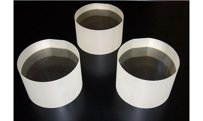
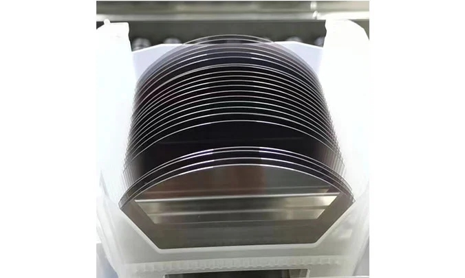
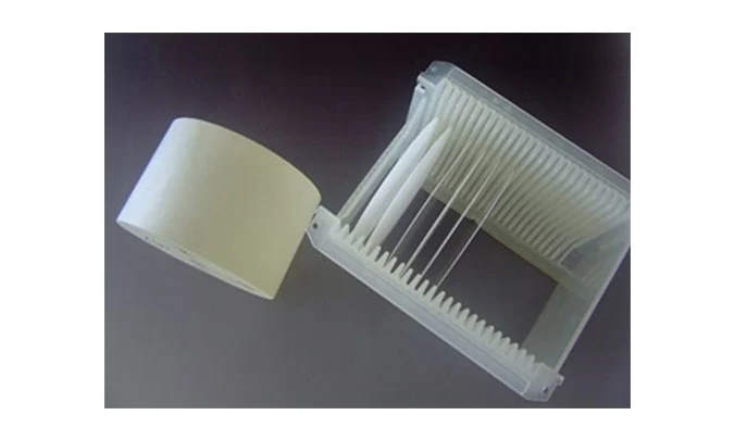
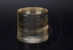
OST Photonics SAW Grade Lithium Niobate Wafers

OST Photonics offers a variety of sizes and thicknesses of SAW grade Lithium Niobate (LiNbO3) wafers, with wafer diameters ranging from 3 inches to 8 inches, the thickness can be customized according to your requirements (generally above 0.18 mm). The orientations can be X/Y/Z/Y36/Y41/Y64/Y128 etc. SAW grade pyroelectric free black lithium niobate wafers(LiNbO3 wafers) are also available upon request.

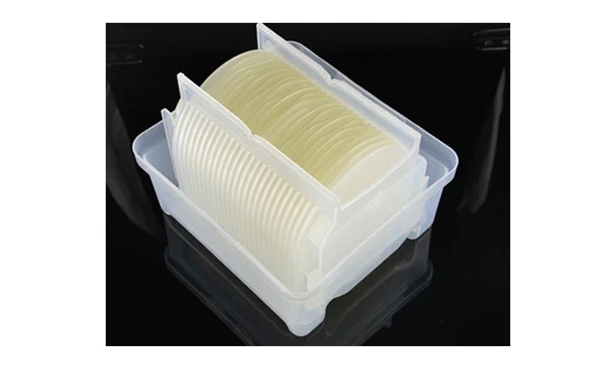
Application of SAW Grade Lithium Niobate Wafers


  • Surfaced acoustic devices

  • Q-switching devices

  • High-performance gyroscope

  • Accelerators and accelerometer sensors

  • MEMS devices


Advantages of SAW Grade Lithium Niobate Wafers


  • Stable mechanical properties

  • Good machinability

  • Heat and corrosion resistance

  • Low cost

  • Easy to grow into large crystals


Ability of SAW Grade Lithium Niobate Wafers


  • Diameter: 3”, 4”, 6”, 8”

  • Orientations: X, Y, Z, Y36, Y41, Y64, Y128 etc.

  • Thickness: 0.25mm, 0.35 mm, 0.5 mm, 1.0 mm etc.

  • Available items: crystal wafers, black reduced wafers, boules, blanks and customized optics


Product parameters of SAW Grade LiNbO3 Wafers


Material

LiNbO3 single crystal

Curie Temp

1142±2.0℃

Reduction

Standard Black - 0.9E+11 ~ 9.0E+11

Super Black - 1.0E+10 ~ 9.0E+10

Cutting Angle

X/Y/Z/Y36/Y41/Y64/Y128 etc

Orientation Tolerance (±)

≤15′

Diameter

3”/4”/6”/8”

Diameter Tolerance (±)

≤0.20 mm

Thickness

0.18 ~ 0.5mm or more

Thickness Tolerance (±)

≤0.025 mm

Primary Flat Length

22mm/32mm/42.5mm/57.5mm

LTV (5mmx5mm)

<1.5 µm

TTV

<1~5 µm

BOW

± (25~40 um)

Warp

<= 35 µm

PLTV(<0.5um)

≥98%(5mm*5mm) with 2mm edge excluded

Orientation Flat

According to our standards or your requests

Surface Type

Single side polished(SSP)/double sides polished(DSP)/double sides lapped(DSL)

Polished Side Ra

<0.5nm

Lapped Side Ra

General is 0.2-0.5 um or as customized

Edge Criteria

Compliant with SEMI M1.2 Standard/refer to IEC62276

Wafer Surface Criteria

Transmissivity

General:5.9x10^-11<s<2.0*10^-10 at 25℃

Contamination

None

Particles φ>0.3 um

<= 30

Scratch , Chipping

None

Defect

No edge cracks, scratches, saw marks, stains

Packaging

Qty/Wafer box

25pcs per box


Product Parameters of SAW Grade LiNbO3 Boules


Material

Grade

Diameter

Growth direction

LiNbO3

SAW

3”/4”/6”/8”

X/Y/Z/Y41/Y64/Y128/Y36/Y etc


Properties of SAW Grade Lithium Niobate Wafers


Growth method

Czochralski method

Crystal structure

M3

Lattice Constant

a=b=5.148 Å     c=13.863 Å

Melting point (℃)

1250

Density(g/cm3)

4.64

Hardness

5 (Mohs)

Refractive index

no=2.286 ne=2.203  at 632.8nm

Nonlinear coefficient

d33=34.45, d31=d15=5.95, d22=13.07 (pmv-1)

Electro-optical coefficient

γ13=8.6, γ22=3.4, γ33=30.8, γ51=28.0, γ22=6.00 (pmv-1)

Optical transmittance

370 ~ 5000nm and >68% at 632.8nm

Thermal expansion

a11=15.4x10^-6/K, a33=7.5x10^-6/K


Related SAW & Optical Grade Lithium Niobate Wafers
Contact Us
Welcome your presence, you can send us an email, we will get in touch with you within 24 hours.
Head Office: No. 66, 8 Group, Chengbei Village, Yanguan Town, Jiaxing 314411, China;

Hangzhou Branch: Room 1012, Chunhua Bussiness Center, No. 159, Hangbo Street, Shangcheng District, Hangzhou 310009, Zhejiang, China
Head Office: No. 66, 8 Group, Chengbei Village, Yanguan Town, Jiaxing 314411, China;

Hangzhou Branch: Room 1012, Chunhua Bussiness Center, No. 159, Hangbo Street, Shangcheng District, Hangzhou 310009, Zhejiang, China
sales@ostphotonics.com; info@ostphotonics.com +86-0571-86780460