E-mail
Jiaxing AOSITE Photonics Technology Co.,Ltd.
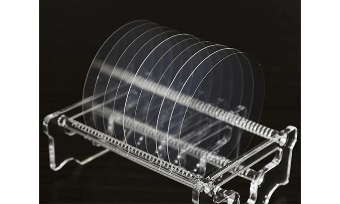
fused silica wafers
fused silica wafers
thin fused silica wafers

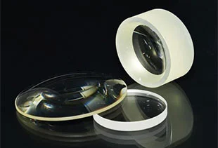
OST Photonics Fused Silica Wafers

OST Photonics offer a variety of optical glass and fused silica wafers depending on the application and material requirements. Wafer diameters are ranging from 3 inch to 12 inch, the thickness can be customized according to your requirements (generally above 0.1 mm). We have a wide range of glass materials for you to choose from:


  • Fused silica material: JGS1/JGS2/JGS3

  • SHOTT glass: Borofloat33/D263Teco/B270(I)/D263(T) and microcrystalline glass etc.

  • Corning glass: Corning 7980/7978/7979 and Eagle XG etc.

  • Ohara glass: SK-1300/SK-1310/SK-1320 etc.

  • Feilihua: F-HUV1~7 etc.

  • CDGM: H-K9L etc.

  • Other glass materials: Soda Lime etc.


Application of Fused Silica Wafers


  • MEMS and electronics industry

  • Semiconductor

  • Biotechnology

  • Integrated circuit (IC) packaging


Advantages of Fused Silica Wafers


  • Excellent light transmittance

  • Low expansion coefficient

  • Strong thermal and impact resistance

  • Excellent chemical stability

  • Good scratch resistance


Ability of Fused Silica Wafers


  • Diameter: 3”, 4”, 6”, 8”, 10”, 12”

  • Material: JGS1/JGS2/JGS3/BF33/D263T/B270(I)/D263(T)/Eagle XG etc.

  • Thickness: 0.1mm, 0.25 mm, 0.5 mm, 1.0 mm etc.

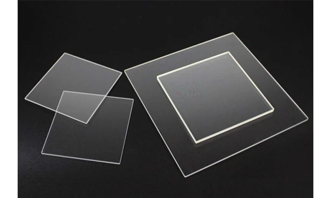
  • Available items: wafers, square plate and customized optics


Product Parameters of Fused Silica Wafers


Material

Fused silica material: JGS1/JGS2/JGS3

SHOTT glass : Borofloat33/D263Teco/B270(I)/D263(T) and microcrystalline glass etc.

Corning glass: Corning 7980/7978/7979 and Eagle XG etc.

Ohara glass: SK-1300/SK-1310/SK-1320 etc.

Feilihua: F-HUV1~7 etc.

CDGM: H-K9L etc.

Other glass materials: Soda Lime etc.

Diameter

3”(76.2mm)

4” (100mm)

6"(150mm)

8"(200mm)

10”(250mm)

12”(300mm)

Diameter Tolerance(±)

≤0.20 mm

Thickness

≥0.1mm

≥0.1mm

≥0.3mm

≥0.4mm

≥0.5mm

≥0.5mm

Primary reference flat

According to our standards or your requests

LTV (5mmx5mm)

< 0.5µm

TTV

< 2µm

< 2µm

< 3µm

<3µm

<5µm

<5µm

Bow

±20µm

±20µm

±30µm

±40µm

±40µm

±40µm

Warp

≤ 30µm

≤ 30µm

≤ 40µm

≤ 50µm

≤ 50µm

≤ 50µm

PLTV(5mm*5mm)<0.4um

≥95%

≥95%

≥95%

≥95%

≥95%

≥95%

Edge Criteria

Compliant with SEMI M1.2 Standard/refer to IEC62276

Surface Type

Single side polished(SSP)/double sides polished(DSP)

Polished side Ra

≤0.5 nm

Back Side Criteria

General is 0.2-0.7µm or as customized

Packaging

25pcs per box


Process Capability of Fused Silica Wafers


Dimension

5mm - 400mm

Thickness

≥0.05mm

Dimensional Tolerance

±25μm

Thickness Tolerance

±5μm

Thickness Variation(TTV)

< 2μm

Flatness

1/10 Wave/Inch

Surface Roughness (RMS)

<5Ǻ

Scratch and Dig

10/5

Particle Size

<10μm

Bow/Warp

<10μm


Contact Us
Welcome your presence, you can send us an email, we will get in touch with you within 24 hours.
Head Office: No. 66, 8 Group, Chengbei Village, Yanguan Town, Jiaxing 314411, China;

Hangzhou Branch: Room 1012, Chunhua Bussiness Center, No. 159, Hangbo Street, Shangcheng District, Hangzhou 310009, Zhejiang, China
Head Office: No. 66, 8 Group, Chengbei Village, Yanguan Town, Jiaxing 314411, China;

Hangzhou Branch: Room 1012, Chunhua Bussiness Center, No. 159, Hangbo Street, Shangcheng District, Hangzhou 310009, Zhejiang, China
sales@ostphotonics.com; info@ostphotonics.com +86-0571-86780460