E-mail
Jiaxing AOSITE Photonics Technology Co.,Ltd.
gallium arsenide substrate

OST Photonics GaAs Substrates

Gallium arsenide (GaAs) is a compound synthesized by two elements of gallium and arsenic. It is an important group IIIA and group VA compound semiconductor material. And it can be used to make microwave integrated circuits, infrared light-emitting diodes, semiconductor lasers and solar cells. GaAs is often used as the base material for the epitaxial growth of III-V semiconductors, including indium gallium arsenide, aluminum gallium arsenide, and so on.


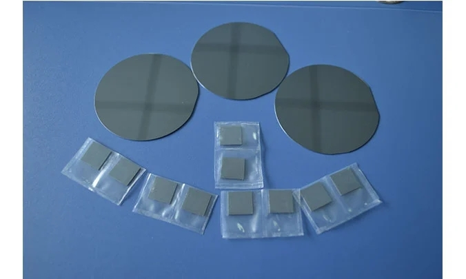
OST Photonics offers high quality GaAs substrates for researchers and industries. There are five types of GaAs materials for you to choose from: semi-insulating GaAs (undoped), N-type GaAs (Si doped), semi-insulating GaAs (Cr doped), N-type GaAs (Te doped) and P-type GaAs (Zn doped). Crystal size and thickness can be customized according to your requirements.

Application of GaAs Substrates


  • Wireless communication

  • Red light LEDs

  • Satellite communications

  • Monolithic microwave integrated circuits (MMIC) for 5G

  • Radio frequency integrated circuits (RFIC)


Advantages of GaAs Substrates


  • Direct band gap

  • High electron mobility

  • High-frequency low noise

  • High conversion efficiency


Ability of GaAs Substrates


  • Orientation:<100>, etc.

  • Dimension: 2”, 3”, 4”, 6”, 25x25mm, 10x10mm, 10x5mm, 5x5mm, etc.

  • Thickness: 0.35mm, 0.5mm, 0.65mm, etc.

  • Available items: wafers, substrates, blanks and customized optics


Specification and Properties of GaAs Substrates


Crystal Structure

Cube

a=5.653 Å

Melting Point

1238 ℃

Density

5.31 g/cm3

Band Gap

1.424

Conduct Type

N-type

P-type

Semi-insulating

Semi-insulating

N-type

Crystal Growth Method

VGF

VGF/LEC

VGF/LEC

VGF

LEC

Dopant

Si

Zn

Undoped

Cr

Te

Carrier Concentration

(0.4-4) ×10^18 /cm3

(0.5-5) ×10^19 /cm3

(0.4-4.4) ×10^8 /cm3

-

(1-2) ×10^17 /cm3

Resistivity

(1.2-9.9) ×10^-3 ohm.cm

-

>1x10^7 ohm.cm

>5x10^7 ohm.cm

(0.74-1.05) ×10^-2 ohm.cm

Mobility

>1000 cm2/v.s

50-120 cm2/v.s

>4000cm2/v.s

5500-6000 cm2/v.s

>1500 cm2/v.s

Etch Pit Density (EPD)

<5000 /cm2

<5000 /cm2

<5000 /cm2

<5000 /cm2

<10000 /cm2

Orientation

<100>, etc.

Orientation Tolerance

±0.5° or better

Dimension

2”, 3”, 4”, 6”, 25x25mm, 10x10mm, 10x5mm, 5x5mm, etc.

Dimension Tolerance

±0.1 mm or better

Thickness

350 μm, 500 μm, 650 μm etc.

Thickness Tolerance

±0.05 mm or better

Surface Finish

Single side polished (SSP)/Double sides polished (DSP)

Surface Roughness

Ra<5Å
Atomic Particle Microscopy (AFM) test report can be provided.

Package

Class 100 clean bag, Class 1000 super clean room


Contact Us
Welcome your presence, you can send us an email, we will get in touch with you within 24 hours.
Head Office: No. 66, 8 Group, Chengbei Village, Yanguan Town, Jiaxing 314411, China;

Hangzhou Branch: Room 1012, Chunhua Bussiness Center, No. 159, Hangbo Street, Shangcheng District, Hangzhou 310009, Zhejiang, China
Head Office: No. 66, 8 Group, Chengbei Village, Yanguan Town, Jiaxing 314411, China;

Hangzhou Branch: Room 1012, Chunhua Bussiness Center, No. 159, Hangbo Street, Shangcheng District, Hangzhou 310009, Zhejiang, China
sales@ostphotonics.com; info@ostphotonics.com +86-0571-86780460