E-mail
Jiaxing AOSITE Photonics Technology Co.,Ltd.
gaas wafer
gaas wafer
gallium arsenide wafer

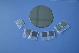
OST Photonics GaAs Wafers

GaAs is a semi-conductor material with excellent performance characteristics including direct band gap, high electron mobility, high-frequency low noise, and high conversion efficiency. The RF devices produced with GaAs substrates are commonly used in wireless communication applications, including wireless networks (WLAN), mobile communication, 4G/5G base stations, satellite communications, and WiFi communications. With the development of mini-LED and micro-LED, red light LEDs produced with GaAs substrates are increasingly used for display screens and in AR/VR.


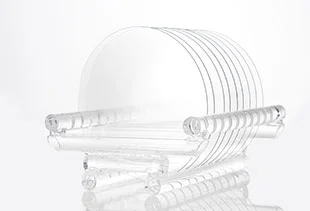
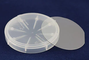
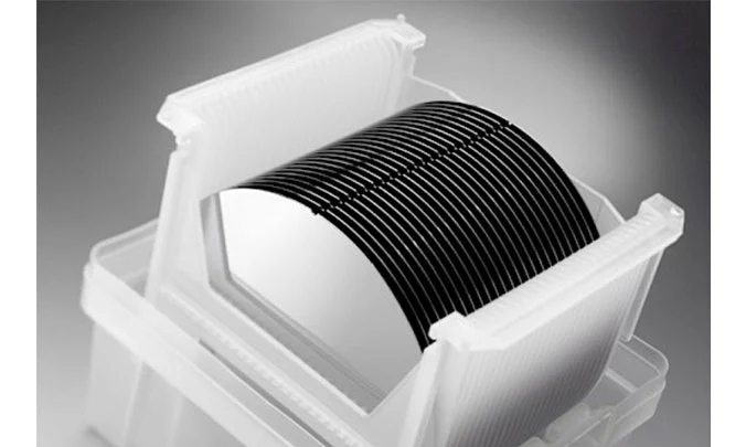
OST Photonics offer 2”, 3”, 4”, 6” GaAs wafers grown by VGF/LEC technology. There are five types of GaAs materials for you to choose from: semi-insulating GaAs (undoped), N-type GaAs (Si doped), semi-insulating GaAs (Cr doped), N-type GaAs (Te doped) and P-type GaAs (Zn doped). The thickness can be customized according to your requirements. In addition, customized GaAs substrates are also available upon requests.

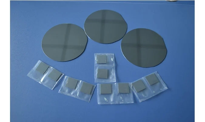
Application of GaAs Wafers


  • Wireless communication

  • Red light LEDs

  • Satellite communications

  • Monolithic microwave integrated circuits (MMIC) for 5G

  • Radio frequency integrated circuits (RFIC)


Advantages of GaAs Wafers


  • Direct band gap

  • High electron mobility

  • High-frequency low noise

  • High conversion efficiency


Ability of GaAs Wafers


  • Orientation:<100>

  • Dimension: 2”, 3”, 4”, 6”, 25x25mm, 10x10mm, 10x5mm, 5x5mm etc.

  • Thickness: 350 μm, 500 μm, 650 μm etc.

  • Available items: wafers, substrates, blanks and customized products


Product Parameters of GaAs Wafers


Item

Specifications

Conduct Type

N-type

P-type

Semi-insulating

Semi-insulating

N-type

Crystal Growth Method

VGF

VGF/LEC

VGF/LEC

VGF

LEC

Dopant

Si

Zn

Undoped

Cr

Te

Carrier Concentration (/cm3)

(0.4-4) ×10^18

(0.5-5) ×10^19

(0.4-4.4) ×10^8

-

(1-2) ×10^17

Resistivity (ohm.cm)

(1.2-9.9) ×10^-3

-

>1x10^7

>5x10^7

(0.74-1.05) ×10^-2

Mobility (cm2/v.s)

>1000

50-120

>4000

5500-6000

>1500

Etch Pit Density (EPD) (/cm2)

<5000

<5000

<5000

<5000

<10000

Dimension

2”, 3”, 4”, 6”

Wafer Orientation

<100>±0.5°

OF/IF

US, EJ or notch

Laser Marking

Upon request

Thickness

350 μm, 500 μm, 650 μm etc.

TTV(P/P) (μm)

≤5

TTV(P/E) (μm)

≤10

Warp (μm)

≤10

Surface

Polished/Polished or Polished/Etched

Epi-ready

Yes

Package

Cassette or single wafer container


Contact Us
Welcome your presence, you can send us an email, we will get in touch with you within 24 hours.
Head Office: No. 66, 8 Group, Chengbei Village, Yanguan Town, Jiaxing 314411, China;

Hangzhou Branch: Room 1012, Chunhua Bussiness Center, No. 159, Hangbo Street, Shangcheng District, Hangzhou 310009, Zhejiang, China
Head Office: No. 66, 8 Group, Chengbei Village, Yanguan Town, Jiaxing 314411, China;

Hangzhou Branch: Room 1012, Chunhua Bussiness Center, No. 159, Hangbo Street, Shangcheng District, Hangzhou 310009, Zhejiang, China
sales@ostphotonics.com; info@ostphotonics.com +86-0571-86780460