E-mail
Jiaxing AOSITE Photonics Technology Co.,Ltd.
gan wafer
gan wafer
gallium nitride wafer

OST Photonics GaN Wafers

Gallium nitride belongs to the third generation of semiconductor material with hexagonal wurtzite structure. It has the characteristics of large forbidden band width, high thermal conductivity, high temperature resistance, radiation resistance, acid and alkali resistance, high strength and high hardness. It has broad application potential and good market prospects in the fields of high-brightness blue, green, purple and white light diodes, blue and purple lasers, and anti-radiation, high-temperature and high-power microwave devices.


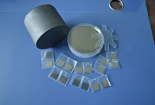
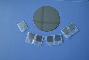
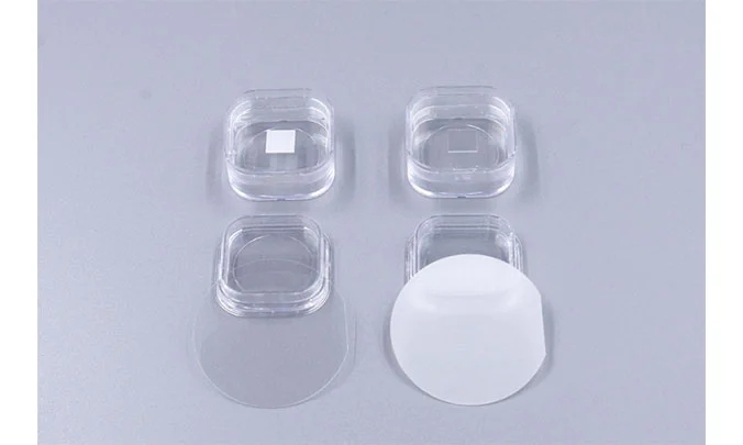
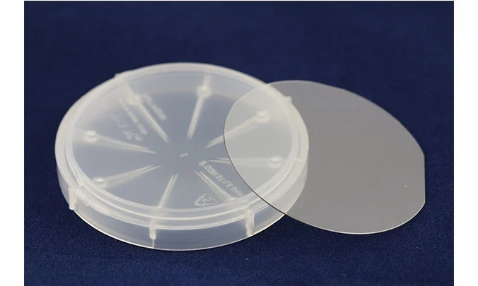
OST Photonics offer free-standing 2” and 4” GaN wafers for semiconductor industry. There are two types of GaN materials for you to choose from: N-type GaN and semi-insulating GaN. Customized GaN substrates and GaN epitaxial on sapphire substrate are also available upon requests.

Application of GaN Wafers


  • High temperature semiconductor device

  • High frequency and high power electronic devices

  • MOS-based devices

  • Ultra-High-Brightness Light Emitting Diode


Advantages of GaN Wafers


  • Large direct band gap

  • Strong atomic bonds

  • High thermal conductivity

  • Strong anti-irradiation ability


Ability of GaN Wafers


  • Orientation: C-plane (0001)

  • Dimension: 2”, 4”, 10x10.5mm, 14x15mm, 10x15mm, etc.

  • Thickness: 300 μm, 350 μm, 400 μm etc.

  • Available items: wafers, substrates, blanks and customized products


Product Parameters of GaN Wafers


Item

Specifications

Diameter

2”, 4”

Thickness

300±25 μm, 350±25 μm, 400±25 μm etc.

Orientation

C-plane (0001)±0.5°

Conduct Type

N-type

Semi-insulating

Resistivity (ohm.cm)

<0.5

>1x10^6

Marco Defect Density (cm-2)

0 or <=2

TTV (μm)

<=15

BOW (μm)

<=20

Dislocation Density (cm-2)

<5x10^6

Useable Surface Area

> 90%

Surface Finish

Front Surface: Ra < 0.2nm (Epi-ready polished)

Back Surface: Fine ground

Package

Packaged in a class 100 clean room environment, in single wafer containers, under a nitrogen atmosphere.


Contact Us
Welcome your presence, you can send us an email, we will get in touch with you within 24 hours.
Head Office: No. 66, 8 Group, Chengbei Village, Yanguan Town, Jiaxing 314411, China;

Hangzhou Branch: Room 1012, Chunhua Bussiness Center, No. 159, Hangbo Street, Shangcheng District, Hangzhou 310009, Zhejiang, China
Head Office: No. 66, 8 Group, Chengbei Village, Yanguan Town, Jiaxing 314411, China;

Hangzhou Branch: Room 1012, Chunhua Bussiness Center, No. 159, Hangbo Street, Shangcheng District, Hangzhou 310009, Zhejiang, China
sales@ostphotonics.com; info@ostphotonics.com +86-0571-86780460