E-mail
Jiaxing AOSITE Photonics Technology Co.,Ltd.
gasb wafer
gasb wafer
gallium antimonide wafers

OST Photonics GaSb Wafers

GaSb single crystals can be used as substrate materials because of their lattice constants matching the lattice constants of various ternary and quaternary, III-V compound solid solutions with band gaps in the 0.8~4.3um wide spectral range. The limited mobility of GaSb lattice is greater than that of GaAs, making it a potential application prospect in the manufacture of microwave devices. Growth methods include LEC, VGF and VBG.


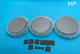
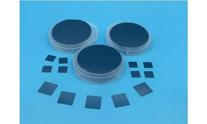
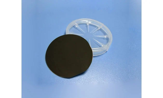
OST Photonics offer 2”, 3” GaSb wafers for semiconductor industry. There are three types of GaSb materials for you to choose from: undoped GaSb, N-type GaSb (Te doped) and P-type GaSb (Zn doped). The thickness can be customized according to your requirements. In addition, customized GaSb substrates are also available upon requests.

Application of GaSb Wafers


  • Optical communication

  • TPV cell

  • Infrared detectors

  • Infrared laser devices


Advantages of GaSb Wafers


  • Low power consumption

  • High electron mobility

  • Wide spectrum coverage

  • Adjustable band width


Ability of GaSb Wafers


  • Orientation:<100>

  • Dimension: 2”, 3”, 10x10mm, 10x5mm etc.

  • Thickness: 500 μm, 600 μm, etc.

  • Available items: wafers, substrates, blanks and customized products


Product Parameters of GaSb Wafers


Item

Specifications

Doping

Undoped

Zn

Te

Conduct Type

P-type

P-type

N-type

Carrier Concentration (cm-3)

(1-2)x10^17

(5-100) x10^17

(1-20)x10^17

Mobility (cm2/V.s)

600-700

200-500

2000-3500

Dislocation Density (cm-2)

<1x10^4

<1x10^4

<1x10^4

Diameter

2”, 3”

Thickness

500±25 μm, 600±25 μm, etc.

Orientation

<100>±0.5°

Surface

Polished/Polished or Polished/Etched

Epi-ready

Yes

Package

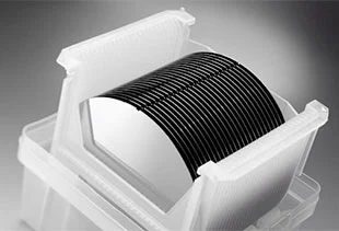
Cassette or single wafer container


Contact Us
Welcome your presence, you can send us an email, we will get in touch with you within 24 hours.
Head Office: No. 66, 8 Group, Chengbei Village, Yanguan Town, Jiaxing 314411, China;

Hangzhou Branch: Room 1012, Chunhua Bussiness Center, No. 159, Hangbo Street, Shangcheng District, Hangzhou 310009, Zhejiang, China
Head Office: No. 66, 8 Group, Chengbei Village, Yanguan Town, Jiaxing 314411, China;

Hangzhou Branch: Room 1012, Chunhua Bussiness Center, No. 159, Hangbo Street, Shangcheng District, Hangzhou 310009, Zhejiang, China
sales@ostphotonics.com; info@ostphotonics.com +86-0571-86780460