E-mail
Jiaxing AOSITE Photonics Technology Co.,Ltd.
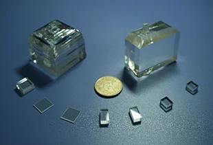
inp substrate
inp substrate
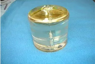
inp crystal

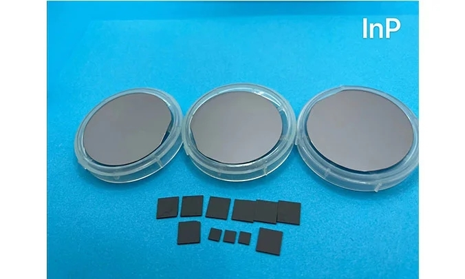
OST Photonics InP Substrates

As one of the most important compound semiconductor materials, InP single crystal materials are key materials for the production of InP-based laser diodes (LD), light-emitting diodes (LEDs) and photodetectors in optical communications. These devices realize the emission of information in optical fiber communications, Dissemination, amplification, acceptance and other functions. InP is also very suitable for high-frequency devices, such as high electron mobility transistors (HEMT) and heterojunction bipolar transistors (HBT). Due to its superior characteristics, it is used in optical fiber communication, microwave, millimeter wave, anti- Many high-tech fields such as radiant solar cells and heterojunction transistors are widely used.


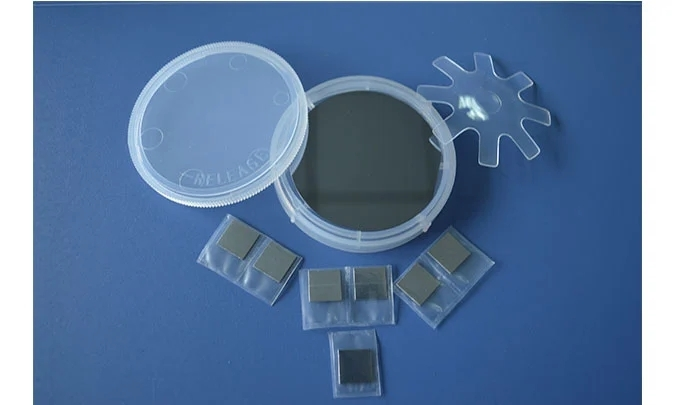
OST Photonics offers high quality InP substrates for researchers and industries. There are four types of InP materials for you to choose from: undoped InP, S-doped InP, Zn-doped InP and Fe-doped InP. Crystal size and thickness can be customized according to your requirements.

Application of InP Substrates


  • RF communication

  • Radar system

  • Radiation survey

  • MEMS


Advantages of InP Substrates


  • High electron mobility

  • Good radiation stability

  • Large band gap


Ability of InP Substrates


  • Orientation:<100>, etc.

  • Dimension: 2”, 3”, 4”, 10x10mm, 10x5mm, etc.

  • Thickness: 0.35mm, 0.5mm, 0.6mm, etc.

  • Available items: wafers, substrates, blanks and customized optics


Specification and Properties of InP Substrates


Crystal Structure

Cube

a=5.869 Å

Melting Point

1600 ℃

Density

4.79 g/cm3

Band Gap

1.344

Conduct Type

Semi-insulating

N-type

N-type

P-type

Dopant

Fe

S

Undoped

Zn

Resistivity (ohm.cm)

≥0.5x10^7

-

Carrier Concentration (cm-3)

-

(0.8-8)x10^18

(1-10)x10^15

(0.8-8)x10^18

Mobility (cm2/v.s)

≥1000

1000-2500

3000-5000

50-100

Etch Pit Density (EPD) (/cm2)

≤5000

≤5000

≤5000

≤500

Orientation

<100>, etc.

Orientation Tolerance

±0.5° or better

Dimension

2”, 3”, 4”, 10x10mm, 10x5mm, etc.

Dimension Tolerance

±0.1 mm or better

Thickness

0.35mm, 0.5mm, 0.6mm, etc.

Thickness Tolerance

±0.05 mm or better

Surface Finish

Single side polished (SSP)/Double sides polished (DSP)

Surface Roughness

Ra<5Å
Atomic Particle Microscopy (AFM) test report can be provided.

Package

Class 100 clean bag, Class 1000 super clean room


Contact Us
Welcome your presence, you can send us an email, we will get in touch with you within 24 hours.
Head Office: No. 66, 8 Group, Chengbei Village, Yanguan Town, Jiaxing 314411, China;

Hangzhou Branch: Room 1012, Chunhua Bussiness Center, No. 159, Hangbo Street, Shangcheng District, Hangzhou 310009, Zhejiang, China
Head Office: No. 66, 8 Group, Chengbei Village, Yanguan Town, Jiaxing 314411, China;

Hangzhou Branch: Room 1012, Chunhua Bussiness Center, No. 159, Hangbo Street, Shangcheng District, Hangzhou 310009, Zhejiang, China
sales@ostphotonics.com; info@ostphotonics.com +86-0571-86780460