E-mail
Jiaxing AOSITE Photonics Technology Co.,Ltd.
crystal substrate
crystal substrate
single crystal substrate

OST Photonics SiC Substrates (4H-SiC, 6H-SiC)

Silicon carbide (SiC) substrate material is an essential material to support the development of the power electronics industry. High purity semi-insulating SiC is mainly used in 5G communication applications. It has the advantages of improving the radio frequency range, ultra-long distance recognition, anti-interference, high-speed and large-capacity information transmission, and is regarded as the most ideal material for making microwave power devices. N-type SiC is mainly used in new energy vehicles, high voltage transmission and transformation stations, white goods, high-speed trains, motors, photovoltaic inverter, pulse power supply and other fields, it has the advantages of reducing equipment energy loss, improving equipment reliability, reducing equipment volume, improving equipment performance and so on, it has irreplaceable advantages in the production of power electronic devices.


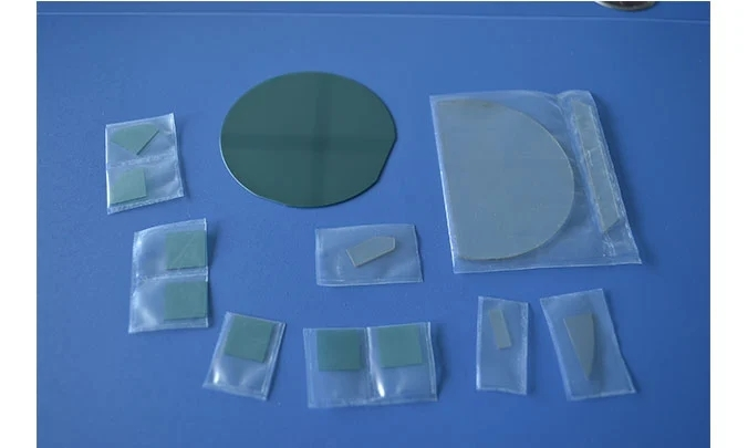
OST Photonics offers high quality SiC(4H-SiC, 6H-SiC) substrates for researchers and industries. Crystal orientation, size and thickness can be customized according to your requirements.

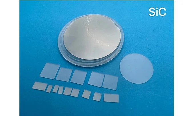
Application of SiC Substrates (4H-SiC, 6H-SiC)


  • 5G Wireless Communication

  • Microwave power device

  • New energy automobile

  • Pulsed power supply

  • Photovoltaic inverter


Advantages of SiC Substrates (4H-SiC, 6H-SiC)


  • Large band gap (about 3 times of Si)

  • High critical field strength (about 10 times of Si)

  • High thermal conductivity (about 3 times of Si)


Ability of SiC Substrates (4H-SiC, 6H-SiC)


  • Orientation:<0001>,<0001>off 4°, etc.

  • Dimension: 4”, 6”, 20x20mm, 15x15mm, 10x10mm, 5x5mm etc.

  • Thickness: 0.33mm, 0.35mm, 0.5mm etc.

  • Available items: wafers, substrates, blanks and customized optics


Specification and Properties of SiC Substrates (4H-SiC, 6H-SiC)


Crystal Structure

Hexagon

Lattice Constant

a=3.08 Å ,c=15.08 Å

Marshalling Sequence

ABCACB (6H), ABCBABCB (4H)

Band Gap

2.93 eV

Hardness

9.2 Mohs

Heat Conductivity @300K

5 W/cm.k

Dielectric Constant

e(11)=e(22)=9.66  e(33)=10.33

Conductor type

SI

N

Dopant

Undoped

Vanadium

Nitrogen

Resistivity

˃1x10^7 ohm.cm

˃1x10^5 ohm.cm

0.01-0.2 ohm.cm

Orientation

<0001>,<0001>off 4°, etc.

Orientation Tolerance

±0.5° or better

Dimension

4”, 6”, 20x20mm, 15x15mm, 10x10mm, 5x5mm etc.

Dimension Tolerance

±0.1 mm or better

Thickness

0.33mm, 0.35mm, 0.5mm etc.

Thickness Tolerance

±0.05 mm or better

Surface Finish

Single side polished (SSP)/Double sides polished (DSP)

Surface Roughness

Ra≤5Å (5µmx5µm)

Package

Class 100 clean bag, Class 1000 super clean room


Contact Us
Welcome your presence, you can send us an email, we will get in touch with you within 24 hours.
Head Office: No. 66, 8 Group, Chengbei Village, Yanguan Town, Jiaxing 314411, China;

Hangzhou Branch: Room 1012, Chunhua Bussiness Center, No. 159, Hangbo Street, Shangcheng District, Hangzhou 310009, Zhejiang, China
Head Office: No. 66, 8 Group, Chengbei Village, Yanguan Town, Jiaxing 314411, China;

Hangzhou Branch: Room 1012, Chunhua Bussiness Center, No. 159, Hangbo Street, Shangcheng District, Hangzhou 310009, Zhejiang, China
sales@ostphotonics.com; info@ostphotonics.com +86-0571-86780460